
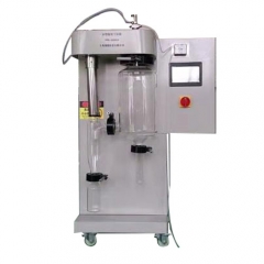
High quality 1.5L scale lab spray dryer equipment
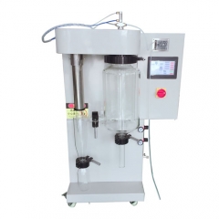
Lab scale spray dryer is suitable for the production of in universities, research institutes and food and pharmaceutical chemical enterprises.
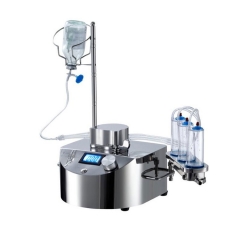
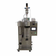
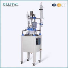
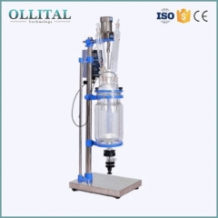
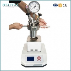
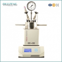
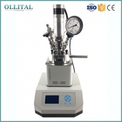
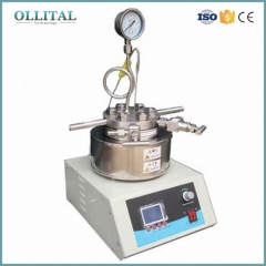
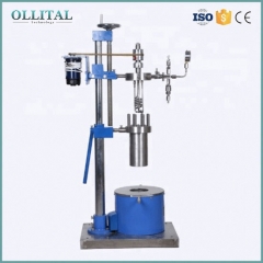
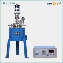
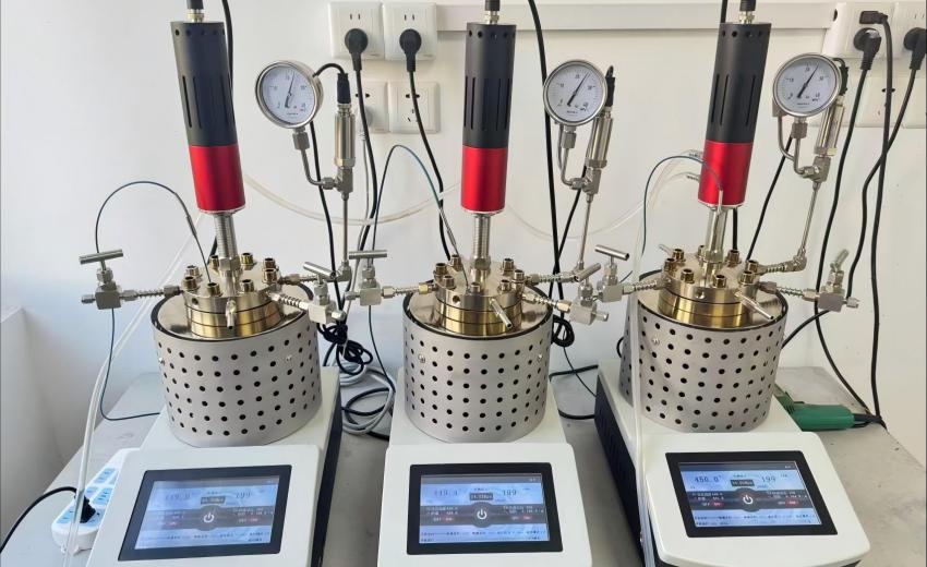
Chemical reactions are often carried out under conditions that cannot be achieved with an ordinary laboratory vessel. When a reaction requires elevate
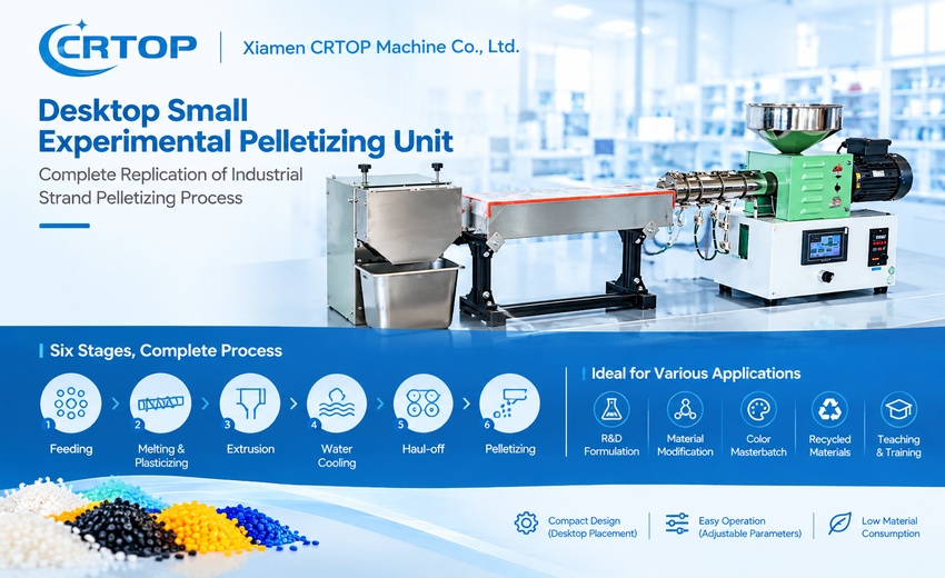
A granulator is a specialized equipment used to process plastic raw materials, modified materials or blended substances into uniform particles. It is

We are pleased to announce another milestone in our overseas market expansion: a batch of high-performance P8 dry ice cleaning machines has been succe
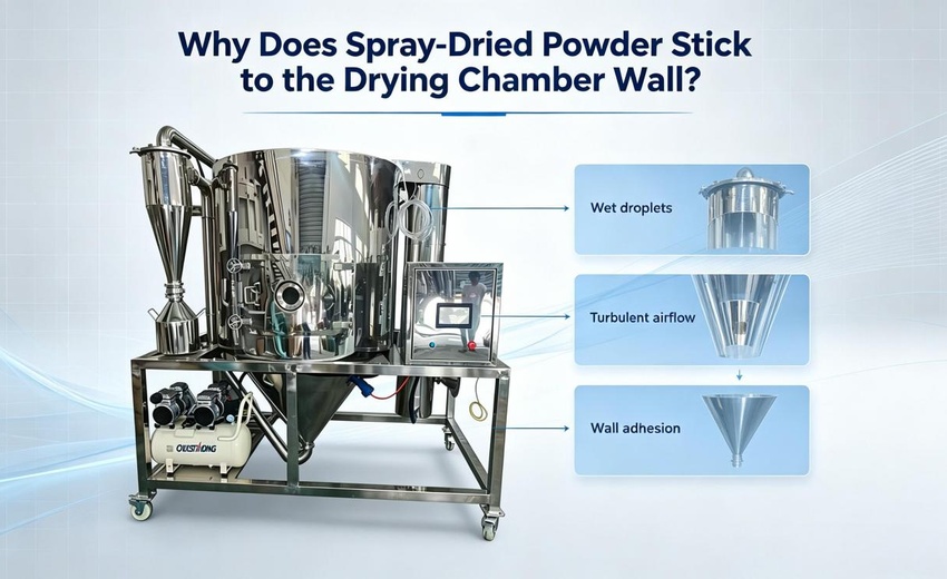
One of the most frustrating problems during spray drying is seeing a large amount of powder stuck to the wall of the drying chamber. The spray dryer m
In the fields of semiconductor, consumer electronics, and precision component manufacturing, surface cleanliness directly determines product yield, performance stability, and service life. As chip fabrication processes shrink to the nanometer scale and electronic components become highly integrated, the limitations of traditional cleaning methods—such as aqueous washing, ultrasonic cleaning, and solvent wiping—have become increasingly apparent. These drawbacks include incomplete cleaning, water residue, damage to precision substrates, incompatibility with micro/nano-scale structures, and environmental pollution from waste liquids.
Against this backdrop, plasma cleaning machines have emerged as essential equipment for semiconductor wafer fabrication, chip packaging, PCB processing, and precision electronic component manufacturing, thanks to their advantages of being dry, non-destructive, high-precision, and capable of cleaning at the nanoscale. They represent a key technology for achieving precision, eco-friendliness, and high efficiency in high-end electronics manufacturing. This article provides an in-depth analysis of the working principles and core advantages of plasma cleaning machines, as well as their mainstream application scenarios and process value within the semiconductor and electronics industries.
Plasma, known as the fourth state of matter, is a highly reactive ionized gas composed of ions, electrons, free radicals, and excited-state molecules. Plasma cleaners operate by using energy sources—such as radio frequency or microwaves—to excite process gases within a vacuum or atmospheric pressure environment, thereby generating a stable, low-temperature plasma. Through the combined effects of physical bombardment and chemical reactions, the system achieves precision cleaning and surface modification at the molecular and nanometer scales without damaging the substrate, delivering an overall cleaning precision in the 3 nm to 30 nm range.
Plasma cleaning processes span the entire manufacturing workflow—from front-end wafer fabrication and mid-end chip packaging to back-end PCB processing and precision electronics assembly—serving as a core technology for ensuring the quality of high-end electronic products.
Wafers serve as the fundamental substrate for chip manufacturing, and an ultra-clean surface is essential for ensuring process precision. During stages such as photolithography, etching, thin-film deposition, and ion implantation, wafers are highly susceptible to residues of photoresist, organic contaminants, metal ions, and surface oxides. Plasma cleaning precisely removes these micro- and nano-scale impurities, ensuring surface flatness and cleanliness. This prevents issues like circuit short-circuits and process deviations caused by contaminants, thereby significantly enhancing manufacturing precision and final product yield. Additionally, plasma treatment activates and modifies the wafer surface, improving the adhesion and uniformity of thin-film and coating depositions.
Chip packaging is a crucial step for ensuring chip stability and represents the most widespread application scenario for plasma cleaning. During processes such as dicing, bonding, and molding, surfaces of leads and bonding pads are prone to accumulating oxide layers, oil stains, and dust. These contaminants can lead to defects such as weak bonding, cold solder joints, packaging delamination, and compromised hermeticity.
Plasma cleaning thoroughly removes oxide layers and organic residues from bonding pads while activating the surfaces of chip leads and substrates. This significantly boosts the bonding strength of gold and copper wires and enhances the adhesion between the molding compound and the chip substrate. It effectively eliminates issues like packaging voids, cracking, and delamination, thereby markedly improving packaging yield and long-term operational stability—making it ideal for the packaging of high-end components such as CPUs, memory chips, and power semiconductors.
During the production of rigid PCBs and flexible FPCs, surfaces, bonding pads, and micro-vias are prone to retaining flux residues, dust, oil stains, and resin powder. Traditional cleaning methods struggle to remove these minute impurities from micro-vias and narrow circuit gaps. Plasma cleaning enables comprehensive, thorough cleaning of the entire circuit board surface—eliminating even microscopic contaminants—thereby resolving issues such as cold joints, weak solder connections, and poor electrical continuity. Additionally, it enhances surface wettability and improves the adhesion of solder masks and adhesives; this effectively protects the board against moisture, oxidation, and corrosion, ultimately boosting the operational stability and service life of the electronic circuitry.
During the bonding processes for mobile phone and tablet OLED/LCD screens and touch panels, microscopic oil residues, dust, and impurities on glass and panel surfaces can lead to air bubbles, adhesive failure, and display defects. Plasma cleaning efficiently removes these micro- and nano-scale surface contaminants and enhances substrate adhesion, resulting in a tighter, more uniform bond with optical adhesives. This significantly reduces defect rates in screen bonding while improving the aesthetic quality and durability of the final product.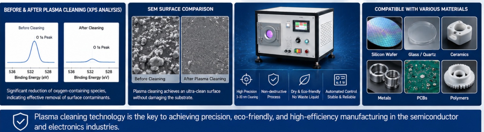
Plasma cleaning has become a standard process in high-end electronics manufacturing. As semiconductor fabrication advances toward 3nm, 2nm, and even more sophisticated nodes, and electronic components rapidly evolve toward miniaturization, integration, high precision, and high reliability, industry demands regarding surface cleanliness, process stability, and eco-friendly production continue to rise. Traditional cleaning methods can no longer meet the requirements of high-end manufacturing, making the shift toward precision plasma dry cleaning increasingly evident. Meanwhile, the widespread adoption of atmospheric-pressure in-line plasma cleaning equipment has resolved the issue of traditional vacuum systems being incompatible with automated production lines; by enabling high-speed, continuous mass production, this technology perfectly aligns with the scale requirements of semiconductor packaging, PCB batch processing, and smart device assembly, establishing itself as a core process choice for high-end semiconductor facilities and electronics manufacturers seeking to improve quality and efficiency while reducing costs and emissions.



 online service
 +86 15960821529
 kevin@ollital.comkevinollital@gmail.com
 +86 15960821529
 +8615960821529


